Difference between revisions of "NailStampPCB"
| Line 71: | Line 71: | ||
# '''Remove''' the scotch tape and use acetone to remove the toner. | # '''Remove''' the scotch tape and use acetone to remove the toner. | ||
# A NEW NAIL STAMP IS BORN! | # A NEW NAIL STAMP IS BORN! | ||
| + | |||
| + | == Results == | ||
| + | [[File:NailStampLaserHSLStamper.jpg|200px]] [[File:NailStampLaserHSLStamperPainted.jpg|200px]] [[File:NailStampLaserHSL.jpg|200px]] | ||
| + | |||
| + | [[File:DIYNailPlate.jpg|200px]] [[File:DIYNailPlateResults.jpg|200px]] | ||
Revision as of 13:58, 14 August 2016
Problem statement
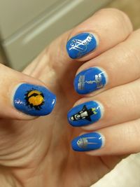
I saw some really cool fingernail decorations online that looked like printed circuit boards. I love and fully endorse the idea of nerd fashion, but I also love DIY. I want to make space nails and use custom logos and designs, like the ISS or the red NASA worm logo.
I bought a silicon nail stamper and some plates from China. It appeared to me that these were probably CNC machined using an engraving bit. There were some really cool designs, and I learned how to stamp them onto nails, which was much more challenging than I thought it would be. I learned the following basic things:
Nail Stamping Lessons Learned
- Use Good Nail Polish I had OK but not great results (the pattern was not very dark) from generic polish. A couple bold colors worked well, like red and silver. I bought some black and white Konad brand stamping polish, which works VERY well.
- Squeegee Technique I got much better results when I painted the entire design than if I painted a stripe and squeegeed across it like many online videos show.
- Squeegee Fast You have to squeegee quickly, but not actually press too hard. The stamper will push tiny extra bits into the cracks if there are small lines.
- Squeegee Lightly If you do press too hard, you will remove too much from larger open areas and get a poor stamp
- Stamp Quickly Speed is everything. Once you squeegee you have a ticking clock. Small lines dry VERY quickly, you have one, maybe two seconds to pick them up.
- Transfer with Haste Once on the stamper, you have about twice as long to transfer the stamp to the nail. It seems that the paint needs to still be tacky to transfer to the nail. If totally dry it will not stick neatly.
- Clear coat in steps The only way I could keep from smearing the stamp while applying clear coat was to paint a single stripe at a time and let fully dry before applying the next stripe. If you wait until you have done all nails first you can just paint one stripe down each nail then circle back around and to the next bit etc. If you in any way drag or interfere with wet clear coat you WILL smear the result. Patience is key!
- Clear Coat Twice A second (or third) , more traditional clear coat on each nail will make the surface look nice and smooth with no stripes.
DIY Idea
The thought occurred to me that maybe, just maybe, a printed circuit board's copper layer would be deep enough to hold enough nail polish for stamping. I performed an experiment using an actual printed circuit board from the junk box. The results were actually remarkably perfect.
DIY PCB Process Using Lasers
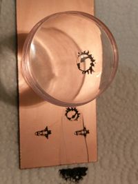
As documented on other pages, I have used the laser engraver at [www.heatsynclabs.org|HSL] to ablate black spray paint from the surface of a copper clad board and follow it up with ferric chloride etchant to remove the exposed copper. I decided that this would be a great place to start. I etched two versions of a small rocket ship and the HSL logo.
- The first step is to prepare the PCB. The board must be cleaned with acetone and allowed to dry, then coated with about three coats of walmart brand flat black paint. This paint is extremely inexpensive at around $1 per can. If only a small area is to be etched, scotch tape can be used to cover large areas of the board. This makes clean up much easier.
- Two engraving passes with the laser (settings were somewhere around 30 watts power, 0.05mm scan gap, 200mm/sec travel) are needed -- the first pass cleans the bulk of the paint and the second pass will remove the re-condensed soot that seems to spray out during the first pass.
- The board is placed directly into the ferric chloride etchant bath and allowed to sit for 5 full minutes.
- Remove the board and dunk into a dilute baking soda bath to neutralize residual etchant on the board.
- Use rubbing alcohol to rub the exposed copper portions of the design with a Q-tip until they are noticeably brighter and the q-tip no longer turns black with soot. This step is required to remove ALL of the soot from the lasered areas and is not optional!
- The board is rinsed with water and placed back into the etchant bath. Constant agitation should be applied to the bath and a back light can be used to check progress.
- Once the light shines through the pattern and the edges of the design look clean, remove the board and dunk back into the backing soda bath.
- Rinse and dry the board. Remove any scotch tape from the board, and use Acetone and paper towels to remove the spray paint mask.
- A NEW NAIL STAMP IS BORN
Results
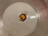
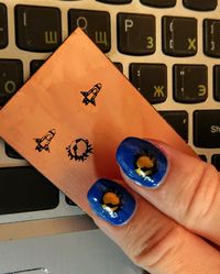
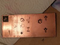
Results of the laser process were nice. Some blurring of the detail was seen, which made the stamps look bold. I liked this. However, one of my main goals in exploring DIY ideas is to find ways to make the technology as accessible as possible, which is a problem because most people do not have access to a CO2 laser and a laser engraver usually costs a lot of money.
DIY Nail Stamps using A Laserjet Printer
I decided to explore the various ways that have been discovered to make PCBs further. The next thing I tried was to print using a laserjet and transfer the toner to the PCB. I will probably not go down the many many many failed pathways, and instead will present two that seemed to work well for me.
Background
I bought some PCB transfer paper, which is like a wax paper. I also tried the same thing using wax paper backing that comes off of shipping labels. I tried using 180 degrees C at 2 minutes under a T-shirt press did a good job of transferring the laserjet mask from the paper to the PCB. I etched these using ferric chloride, and had good results. But A T-shirt press is actually not a very common thing, and is still pretty expensive.
Since most every home has a clothes iron, I tried about 594808374589 times to use my clothes iron to transfer the printed image from about 3945 types of paper to the PCB. I never had a single good usable transfer. Some of them looked OK, but upon inspection I realized that the paper had either moved, or been squished by the pressure and distorted the pattern. I was not able to make a clothes iron work.
A quick search of the internet showed that a TL901C-T laminator could be acquired for only $29. This is not a lot of money and is within most people's financial reach if they can also afford quality nail polish in the first place. I have had VERY good success with this laminator on the 5-mil setting using scotch tape to hold the leading edge of the paper to the PCB as fed into the laminator, and making sure that the paper is smaller than the overall dimensions of the PCB.
Step-by-step
- Find a *REAL* LASER JET (NOT AN INKJET) PRINTER
- Clean the PCB with acetone.
- Prepare your nail art on the PC. I find that 10mm is the largest dimension that will cover a thumbnail, and 6-8mm is the largest dimension that will cover a fingernail. Don't forget to mirror the design from left to right!
- The pattern should be white art on a black square just larger than the art. Most times you can just invert a black and white image in paintbrush to get this effect, or you can use inkscape (which is what I use).
- Lines should be at least 0.2mm (maaaaybe 0.18mm if needed) or wider. Smaller lines don't really stamp or etch well.
- Print onto Mary Kay magazine pages, or other glossy magazine pages that arrive as junk mail. Do not use the covers, however.
- Turn the printer settings to darkest, which will deposit the most toner. Turn off eco settings or other toner saver settings.
- On my laserjet, there is a setting for 'rough' paper. I use the 'rough 1' setting, but you should explore which settings make the best image on the paper before proceeding.
- Cut out the print leaving a small border of paper around the black print. Do not touch the print itself!!!
- Gently place the paper onto a blank portion of your PCB, making sure that the paper isn't off any edges of the PCB
- Secure the leading edge with a piece of scotch tape
- Feed the PCB, scotch tape edge first and laminate 10 times back to back as quickly as possible
- Being careful of the now very toasty pcb board, place it under the sink and start a very light cold water flow directly on top of the center of the pattern.
- Rinse the paper for 3 minutes.
- Gently peel the paper and scotch tape off of the board. If you did this correctly, the paper will come apart and leave the toner design behind. Do not touch the deisign.
- Use a Q-tip under the water flow to gently scrub away the paper fibers. You will see the design slowly turn black as the paper is removed. Once complete, let dry but DO NOT TOUCH THE TONER!!
- Cover the portions of the board that you do not want to etch with scotch tape
- Use a Q-tip to lightly apply a few drops of ferric chloride and *very gently* wipe with the Q-tip for about 10 minutes, adding new drops as the liquid becomes dark.
- OR if you are doing many designs at once, submerge the board into an etchant bath and agitate.
- I use a back light to determine when the design has fully removed the copper
- Once done, dip the board into a baking soda bath, then rinse in the sink
- Remove the scotch tape and use acetone to remove the toner.
- A NEW NAIL STAMP IS BORN!
