Difference between revisions of "HiSpeedFlash"
(Added ringdown pic) |
(Added Schematic) |
||
| Line 10: | Line 10: | ||
===Electronics Design === | ===Electronics Design === | ||
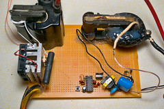
The supporting electronics consist of power converters of the flyback topology running off of scrounged parts and 555 timers. All values were experimentally determined using a function generator to drive the switching transistor, and then transferring the parameters to the 555 circuits. The main circuit switches power into a flyback transformer from a TV set to charge the main capacitor bank. Another power converter feeds a voltage doubler which charges the trigger capacitor to approximately 400 volts. This capacitor is triggered using a thyristor to discharge into another flyback transformer from a TV set to provide the ~45kv gate voltage required to drive the flash bulb. | The supporting electronics consist of power converters of the flyback topology running off of scrounged parts and 555 timers. All values were experimentally determined using a function generator to drive the switching transistor, and then transferring the parameters to the 555 circuits. The main circuit switches power into a flyback transformer from a TV set to charge the main capacitor bank. Another power converter feeds a voltage doubler which charges the trigger capacitor to approximately 400 volts. This capacitor is triggered using a thyristor to discharge into another flyback transformer from a TV set to provide the ~45kv gate voltage required to drive the flash bulb. | ||
| − | <flickr>307586883|left|thumb|m|The control electronics</flickr><br clear="all"/> | + | <flickr>307586883|left|thumb|m|The control electronics</flickr> |
| + | <flickr>4790187233|none|thumb|m|Quick N Dirty Schematic</flickr><br clear="all"/> | ||
===Updated Design In 2010 === | ===Updated Design In 2010 === | ||
| Line 32: | Line 33: | ||
<embed src="http://www.flickr.com/apps/slideshow/show.swf?v=71649&offsite=true&lang=en-us&page_show_url=%2Fphotos%2Fnebarnix%2Fsets%2F72157594248654650%2Fshow%2F&page_show_back_url=%2Fphotos%2Fnebarnix%2Fsets%2F72157594248654650%2F&set_id=72157594248654650&jump_to=" width="800" height="400"></embed> | <embed src="http://www.flickr.com/apps/slideshow/show.swf?v=71649&offsite=true&lang=en-us&page_show_url=%2Fphotos%2Fnebarnix%2Fsets%2F72157594248654650%2Fshow%2F&page_show_back_url=%2Fphotos%2Fnebarnix%2Fsets%2F72157594248654650%2F&set_id=72157594248654650&jump_to=" width="800" height="400"></embed> | ||
| − | + | 2012 Jasper Nance KE7PHI | |
Latest revision as of 13:20, 27 February 2014
Problem statement
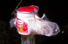
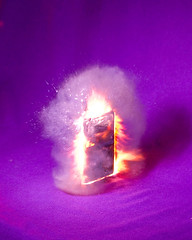
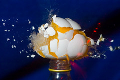
I want to photographically capture a bullet in flight, as well as other similarly timed events such as explosions. I want the flash duration to be somewhere on the order of ~1uS. Shorter is better but I want to be able to shoot at 100-200 ISO speed at F5.6-8.0 for maximum depth of field and sharpness.
Device Description
Bulb Design
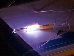
The flash bulb is essentially a field effect transistor (FET). The channel is atmospheric air and is approximately 1 inch long to set a breakdown voltage of around 20KV. The gate is made of quartz, approximately 1/8 inch thick. The applied gate voltage is ~45kv. A capacitor bank is charged to 18KV DC and held across the channel until the gate pulse ionizes the air in the channel and conduction begins. The capacitor bank was roughly 35nF (later increased to 56nF) and it made up of 10Kv 11nF capacitors in parallel and series to form a 20KV rated maximum voltage. Inductance is minimized by stacking the capacitors into 'hockey puck' shaped layers with aluminum foil sandwiched between.
Electronics Design
The supporting electronics consist of power converters of the flyback topology running off of scrounged parts and 555 timers. All values were experimentally determined using a function generator to drive the switching transistor, and then transferring the parameters to the 555 circuits. The main circuit switches power into a flyback transformer from a TV set to charge the main capacitor bank. Another power converter feeds a voltage doubler which charges the trigger capacitor to approximately 400 volts. This capacitor is triggered using a thyristor to discharge into another flyback transformer from a TV set to provide the ~45kv gate voltage required to drive the flash bulb.
Updated Design In 2010
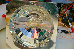
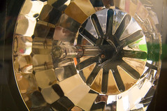
The previous design had some serious flaws not the least of which was the nasty reflector. A redesign effort was made using a new LED strobe light reflector and body (minus guts). The result is a clean focused light pattern with no chance of accidental arcing to the reflective paint (which causes vaporazation, crazing, and clouding). A test tube covering the discharge tube was found to be essentail to prevent metal vapor from condensing onto the reflective surface rendering it cloudy and quite blue tinted.
The capacitor bank was also upgraded from a massive array of rolled russian capacitors to a single 30nF 35kV Maxwell Pulse cap. The pulse capacitor is specifically designed to be low inductance. The reduction in capacitance is more than made up by supplying a higher voltage, ~27kV was coaxed out of the flyback transformer. This blew out the HV diode inside of the transformer, but the addition of a 30KV external diode string has returned the power supply to operation.
Discharge Profile and Flash Duration
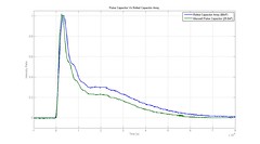
The flash duration is around 500nS with some extended ringdown due to the inductance of the lead wires. Using copper strap would go a long way towards reducing that.
Example photographs
Slideshow of Highspeed Photographs
<embed src="http://www.flickr.com/apps/slideshow/show.swf?v=71649&offsite=true&lang=en-us&page_show_url=%2Fphotos%2Fnebarnix%2Fsets%2F72157594248654650%2Fshow%2F&page_show_back_url=%2Fphotos%2Fnebarnix%2Fsets%2F72157594248654650%2F&set_id=72157594248654650&jump_to=" width="800" height="400"></embed>
2012 Jasper Nance KE7PHI
